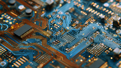
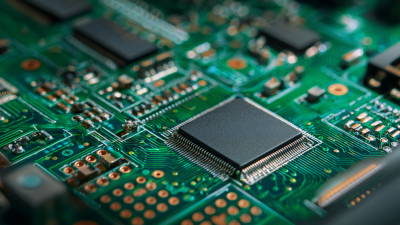
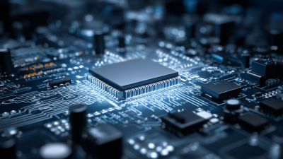
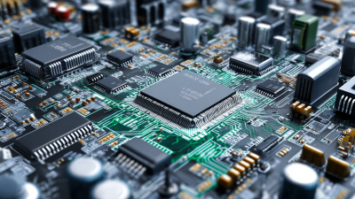
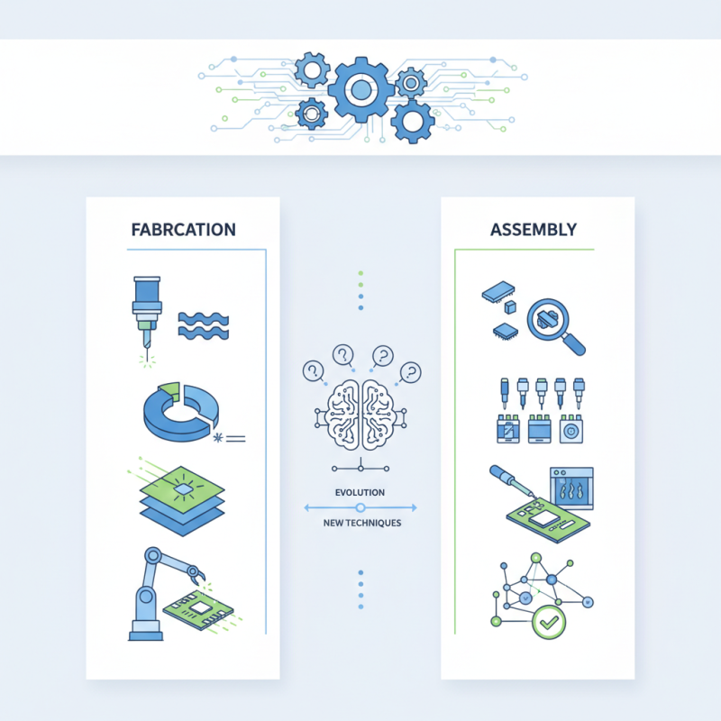
In the rapidly evolving world of electronics, understanding PCB fabrication and assembly is crucial. These processes are at the heart of every electronic device we use. From smartphones to medical equipment, PCBs serve as the backbone, connecting various components.
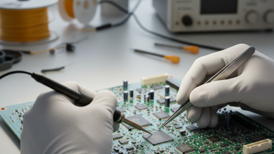
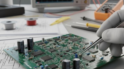
Each fabrication technique has its own nuances. Some methods prioritize speed, while others focus on precision. This makes choosing the right technique a challenge. Mistakes in PCB fabrication can lead to costly errors. Assembly processes are equally vital, requiring meticulous attention to detail. A minor oversight can disrupt the entire product.
It's essential to stay informed about the latest trends in PCB fabrication and assembly. As technology advances, new techniques emerge that offer improved efficiency. However, with innovation comes complexity. Understanding both the advantages and potential pitfalls of each method is key.
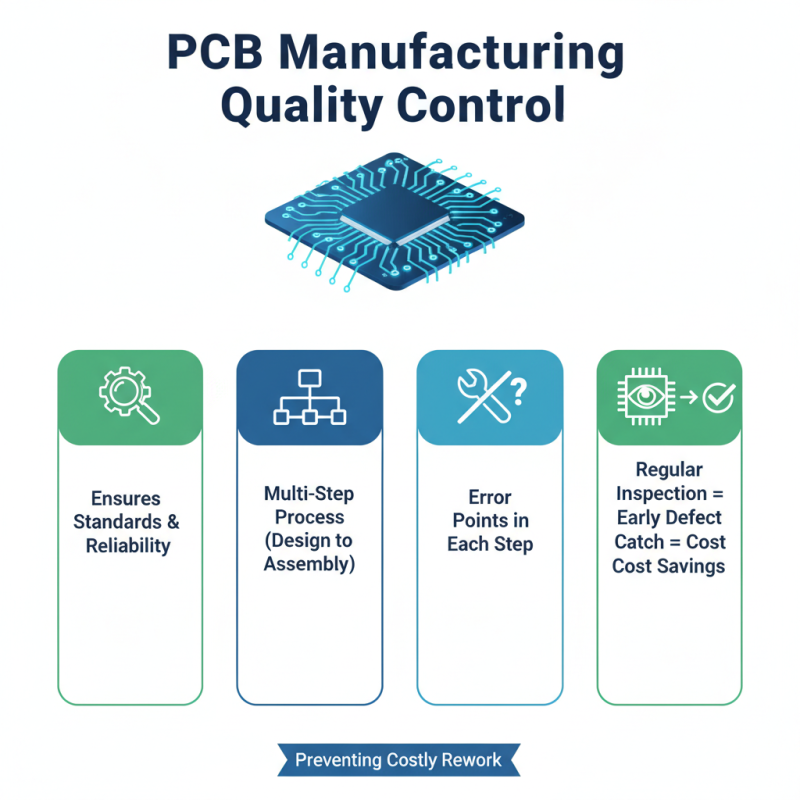
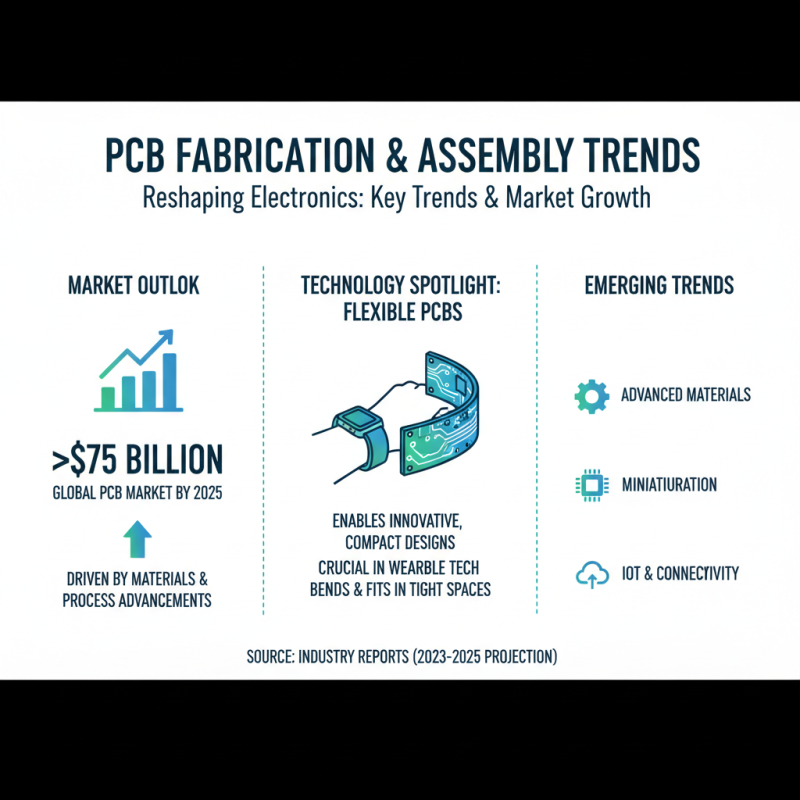
Understanding PCB fabrication processes is essential for anyone in the electronics industry. These processes directly impact performance, reliability, and cost. According to IPC, the global PCB market is projected to reach $70 billion by 2026. This signals growing demand. However, many manufacturers still struggle with quality control during these processes.
One critical fabrication technique is photolithography. This method uses light to transfer patterns onto the PCB layer. This process can produce intricate designs. Data shows that over 30% of defects arise during this phase. Companies often overlook this risk, prioritizing speed over precision. Another crucial step is etching, where unnecessary copper is removed. Inadequate etching can lead to weak connections, resulting in device failures.
Furthermore, assembly processes like surface mount technology (SMT) have gained traction. SMT allows for miniaturized components. A report by Research and Markets estimates that SMT will dominate the PCB assembly segment by 2025. However, the rapid pace of innovation can lead to misalignment in components. This highlights the need for stringent inspection methods to ensure quality. Understanding these nuances can dramatically affect product outcomes in the long run.
When exploring PCB component assembly methods, one can encounter a variety of techniques that cater to different project needs. Surface mount technology (SMT) is one of the most common processes today. It allows for components to be mounted directly onto the surface of the PCB. This method offers a variety of advantages, including space efficiency and the ability to support automated assembly.
Another notable method is through-hole assembly, which involves inserting components through holes in the PCB. While this technique is often seen as outdated, it remains essential for specific components that require more robust mechanical connections. The transition between these methods can be challenging. Designers must balance factors such as cost, size, and the specific application of the PCB. Many engineers find themselves in a bind when trying to choose the best method for their needs.
Flexibility in manufacturing is crucial. For complex PCBs with varying sizes and shapes, multi-layer PCB assembly can be quite useful. However, handling varying thicknesses and soldering techniques can lead to inconsistencies. Mistakes in alignment or miscalculations in pad sizes may occur, leading to defective assemblies. Reflection on these challenges is necessary for improving processes in the future. Each method has its trade-offs, making careful consideration essential for successful PCB assembly.
The optimization of PCB design and layout is critical for enhancing performance and reducing costs. According to a report by IPC, effective layout can lead to a 20% decrease in production costs. One key technique is the placement of components. Intelligent placement minimizes trace lengths, which reduces signal degradation. However, novice designers often overlook this, resulting in longer traces and potential interference.
Another critical aspect is the use of ground planes. Ground planes help to mitigate electromagnetic interference. A study showed that PCBs with optimized ground planes had a 30% improvement in signal integrity. Still, many fail to utilize this technique effectively. This can lead to increased noise and performance issues.
Design rules should never be ignored. Designers must adhere to spacing and sizing guidelines to prevent issues. While software tools help with these rules, human oversight remains vital. A lack of attention can lead to costly mistakes. Tight deadlines often push designers to compromise on these essential checks. A balance is needed between speed and accuracy in the design process.
| Technique | Description | Benefits | Common Applications |
|---|---|---|---|
| Surface Mount Technology (SMT) | A method to mount electronic components directly onto the surface of a PCB. | High component density, automated assembly, reduced production costs. | Consumer electronics, computers, communications devices. |
| Through-Hole Technology | Components are inserted into holes drilled in the PCB and soldered on the opposite side. | Strong mechanical bonds, easier to repair. | Industrial machines, high-power applications. |
| Via Plating | The process of coating the inside of holes with conductive material to create electrical pathways. | Improved connectivity, reduced manufacturing costs. | Multilayer PCBs, complex circuit designs. |
| Solder Masking | A protective layer applied to the PCB to prevent solder bridging and corrosion. | Enhanced durability, improved aesthetics. | All types of electronic devices. |
| Global Positioning System (GPS) Integration | Incorporating GPS technology for location tracking in devices. | Adds functionality to devices, improves navigation accuracy. | Automobiles, mobile devices, drones. |
| Automated Optical Inspection (AOI) | Utilizing cameras to inspect PCBs for defects during production. | Increased quality control, early defect detection. | Manufacturing processes, quality assurance. |
| Design for Manufacturing (DFM) | Designing PCBs considering the manufacturing process to reduce costs and improve efficiency. | Lower production costs, fewer manufacturing issues. | All PCB types. |
| RFC (Radio Frequency Circuit) Design | Special design considerations for circuit boards that operate at radio frequencies. | Optimized signal integrity, reduced interference. | Telecommunications, wireless devices. |
| Thermal Management Techniques | Strategies to manage heat dissipation in high-power electronics. | Improved device reliability, enhanced performance. | Power supplies, LED lighting, automotive applications. |
| Flexible Printed Circuits (FPC) | PCBs made from flexible materials that can bend and twist. | Space-saving designs, lightweight, increased design flexibility. | Wearable technology, foldable devices, automotive controls. |
Quality control in PCB manufacturing is crucial. It ensures that products meet industry standards and function reliably. The manufacturing process involves several steps, from design to assembly. Each step is an opportunity for errors to occur. Regular inspections can catch defects early. This helps avoid costly rework later.
Visual inspection is one common practice. Operators look for solder issues or component misalignment. Automated Optical Inspection (AOI) can also help. It uses cameras to check for defects. However, relying solely on technology can be risky. Human oversight is still necessary to catch subtle problems.
Testing is another key aspect of quality control. Functional tests expose boards to conditions they will face in real use. Some boards may pass visual inspection but fail functional tests. This is where reflection is vital. Are your testing practices thorough enough? Continuous improvement in quality control processes can lead to better end products. Regular training for staff on quality standards is also essential.
Emerging trends in PCB fabrication and assembly technologies are reshaping the electronics industry. Industry reports indicate that the global PCB market is expected to reach over $75 billion by 2025, driven by advancements in materials and processes. One significant trend is the use of flexible PCBs. These boards enable innovative designs that can bend and fit into compact spaces. Flexible PCBs are becoming crucial in wearable technology.
Additionally, advanced automation in PCB assembly is gaining traction. Automation can increase production speed and reduce errors. A survey noted that 70% of manufacturers are investing in automated assembly solutions. However, the initial investment can be high. Not every company can afford this upfront cost, which may widen the gap between large corporations and smaller firms.
Sustainability is also a growing concern. Many companies are seeking eco-friendly materials and processes. There's an increasing demand for recycling technologies in PCB manufacturing. Yet, the processes are not fully developed. There is still much work needed to improve efficiency in material recovery. Integrating these emerging trends presents challenges and opportunities for manufacturers worldwide.