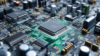
How to Successfully Create a PCB Assembly Prototype for Your Project?
Creating a successful PCB assembly prototype is essential for any electronics project. In today's fast-paced market, companies cannot afford costly mistakes. According to a recent industry report by IPC, nearly 40% of PCB prototypes fail due to design issues. This highlights the importance of a thorough development process.
Dr. Emily Lin, a recognized expert in electronic manufacturing, emphasizes, “The success of a project largely depends on the quality of its initial PCB assembly prototype.” Her insights remind us that meticulous planning is crucial. Without proper attention to detail, teams can encounter setbacks that delay project timelines and inflate budgets.
Iterative testing is a key element in refining prototypes. Designers must be prepared to accept imperfections and think critically about each version they produce. Learning from each prototype can lead to better overall designs, ultimately enhancing product performance in the competitive electronics market. A well-crafted PCB assembly prototype can make all the difference.
Understanding the Basics of PCB Design for Prototyping
When creating a PCB assembly prototype, understanding the basics of design is crucial. Start with a clear circuit schematic. This diagram serves as your blueprint. It should represent all components and their connections. If the schematic is unclear, the prototype will likely fail. Pay attention to component placement. Consider how the layout affects signal flow and heat dissipation. The wrong arrangement can lead to performance issues.
After establishing the schematic, move to PCB layout. Choose the right dimensions for your project. Prototyping often requires iterative adjustments. You may find that your first draft doesn't fit well. Don’t hesitate to make changes. Utilize design software to visualize your ideas. Check for errors before committing to production. Errors like trace width and spacing can greatly impact functionality.
Testing the prototype is essential. Sometimes, components behave unexpectedly. Be prepared for adjustments based on real-world usage. Reflect on failures to improve your design process. Each iteration will teach valuable lessons. Engaging in this cycle will enhance your skills and results. Prototyping isn't just technical; it’s also a journey of learning and growth.
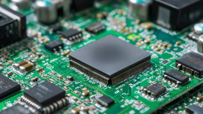
Choosing the Right Materials and Components for Your PCB Prototype
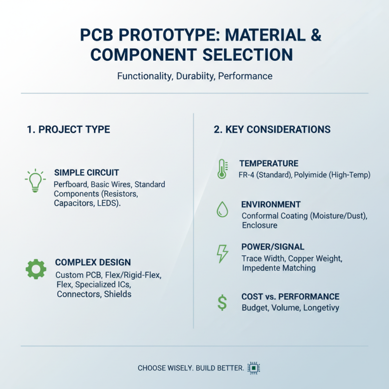
Choosing the right materials and components for your PCB prototype is crucial. The choice determines functionality, durability, and overall performance. Start by considering the type of project. Are you building a simple circuit or something complex? Different projects require different approaches.
Materials like copper, epoxy, and FR4 are common in PCB fabrication. Copper thickness affects conductivity. Thicker copper can carry more current but may be more expensive. Evaluate your project's needs versus budget constraints. Choosing suboptimal materials can lead to failures.
Components must also align with your design requirements. Resistances, capacitors, and microcontrollers need careful selection. Consider their ratings and tolerances. It’s tempting to go for the cheapest options, but this can impact performance. It’s wise to test a few components before settling. A trial and error approach can be enlightening but also frustrating. Embrace that learning process—it often leads to valuable insights.
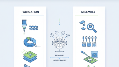
Step-By-Step Process of Designing a PCB Layout
Designing a PCB layout requires careful planning and execution. Start with brainstorming your project requirements. Identify key components, their size, and functionalities. The layout should accommodate all necessary parts while ensuring proper connectivity. Research shows that nearly 70% of PCB design errors come from inadequate planning.
Once you have a rough sketch, move on to schematic capture. Use industry-standard design tools to create diagrams. This process validates electrical connections. Pay attention to signal integrity and power distribution. According to a report by IPC, faulty layouts are responsible for 50% of PCB failures. Therefore, simulation and analysis play a crucial role.
After schematic completion, begin the actual layout design. Position components logically to minimize trace lengths. Consider placement's impact on thermal management. Space is vital; overcrowding increases failure risks. When laying out traces, aim for 15 mils for standard traces. It may seem simple, yet oversights can lead to significant problems. Regular reviews during this phase can help spot errors early. Creating a functional PCB prototype is an iterative process requiring patience and attention to detail.
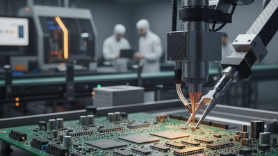
Techniques for Effective PCB Assembly Methods
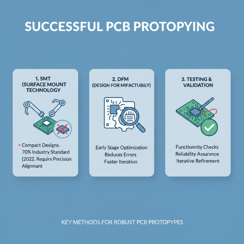
Creating a successful PCB assembly prototype involves multiple effective methods. One critical technique is the use of surface mount technology (SMT). According to a 2022 industry report, SMT has become the preferred method for about 70% of assembly processes. This technique allows for smaller components, which leads to more compact designs. However, misalignment can occur during placement, leading to defects. Attention to detail during this step is crucial.
Another important aspect is selecting the right soldering technique. In 2023, an analysis showed that nearly 75% of defects are related to soldering issues. Reflow soldering is commonly used for SMT components. Yet, it requires precise temperature control. Too high or too low can cause solder bridges or cold joints. Regular monitoring of the reflow profiles is essential to avoid these pitfalls.
Component testing throughout the assembly process is also vital. A study revealed that early detection of faults reduces overall project timeline by up to 30%. Implementing in-circuit testing can catch issues before progressing. It's imperative to remember that skipping any testing phase increases risk. The goal should always be to refine each stage, aiming for a prototype that meets both functionality and quality standards.
Testing and Troubleshooting Your PCB Prototype Before Finalizing
Testing your PCB prototype is crucial. Start by verifying the design. Use a multimeter to check connections. Make sure each component is in place. Look for any misplaced parts. A simple visual inspection can save hours.
Next, power up the board. Monitor it closely. Look for smoke or unusual heat. If something feels off, turn it off immediately. You're looking for real-world issues. Sometimes, a feature might not function as expected. That’s a signal something is wrong.
Troubleshooting can be frustrating. Use systematic methods to identify the problem. Try isolating different sections of the circuit. Check each part one by one. Document your findings. This step is often overlooked but vital. Recognizing what you did wrong helps you improve. Avoiding similar mistakes is key to progress.
PCB Assembly Prototype Testing Results