What is a PCB Board and How is it Used in Electronics?
In the heart of modern electronics lies the PCB board, a crucial component in countless devices. Experts agree that the importance of PCB boards cannot be overstated. David Chen, a renowned engineer in the electronics field, once stated, "PCB boards are the backbone of electronic design; they facilitate connectivity and performance." This highlights their role in both simple gadgets and complex machinery.
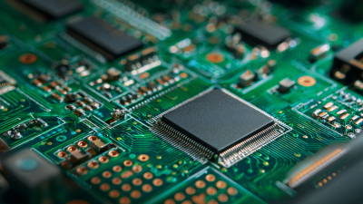
A PCB board, or printed circuit board, serves as a platform for arranging electronic components. It connects various parts of a circuit, ensuring they work together seamlessly. From smartphones to home appliances, PCB boards are integral to the functionality of these devices. However, the manufacturing process must be precise. Even a minor flaw can lead to significant issues, emphasizing the need for quality assurance.
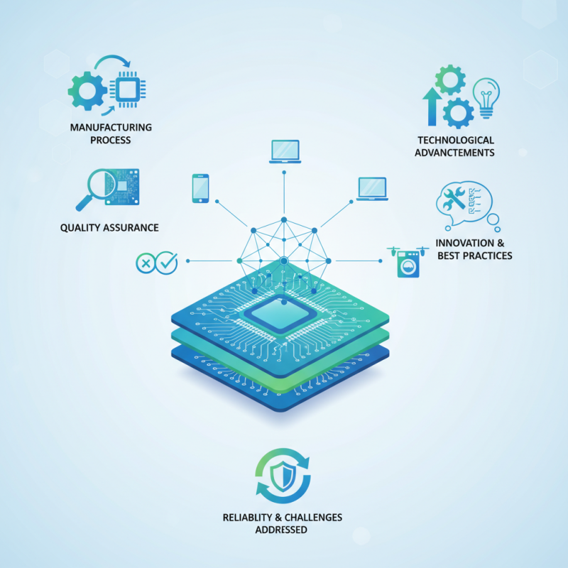
Despite their essential role, the field is not without challenges. Rapid technological advancements push manufacturers to innovate constantly. This rapid pace can sometimes lead to oversights. As the industry evolves, staying updated with best practices is vital. Manufacturers must reflect on their processes to maintain the reliability of their PCB boards. Addressing these challenges ensures the ongoing effectiveness of these essential components.
What is a PCB Board?
A PCB board, or printed circuit board, is an essential component in modern electronics. It provides a structured platform for connecting electrical components. Made from layers of insulating material and conductive pathways, PCBs create circuits that power devices like smartphones, computers, and appliances. Their design allows for compact and efficient layouts, maximizing the use of space in electronic devices.
When considering how PCBs are created, one might reflect on the complexities involved. A simple mistake in the design process can lead to poor functionality. It's crucial to ensure that all connections are properly aligned. Tips for designing a reliable PCB include using clear schematics and verifying every step of the layout. Check component placements regularly to avoid costly errors.
PCB boards can vary widely in complexity. Some contain just a few components, while others may have hundreds. This variability poses unique challenges for engineers. They must adapt their approach based on the project's specific needs. Always remember that testing is key. Conduct thorough tests in multiple conditions to ensure durability and reliability over time. Regular reviews and updates of designs can prevent unforeseen issues.
Usage of PCB Boards in Electronics
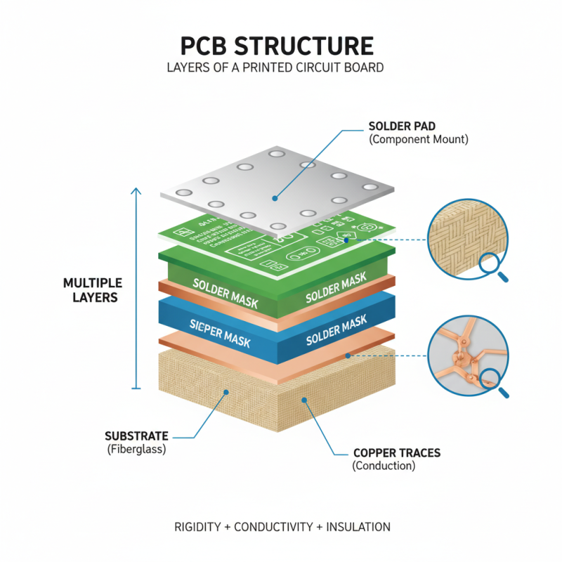
The Structure and Layers of a PCB Board
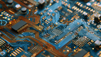
A PCB board, or printed circuit board, is a crucial component in modern electronics. Understanding its structure helps us grasp its functionality. A typical PCB consists of multiple layers. The base material is usually fiberglass. It provides rigidity and stability. The layers serve different purposes, from conducting electricity to providing insulation.
Trace layers are essential. These copper paths connect different components like resistors and capacitors. The thickness of these traces impacts performance. There’s also a layer for solder mask, which prevents short circuits. This layer is usually green, but colors can vary. Finally, the silkscreen layer holds markings and labels to guide assembly.
While the construction seems straightforward, challenges can arise. Misalignment during layering can lead to failures. Design mistakes may cause performance issues too. Engineers must pay close attention to details. Even small errors can lead to malfunction, affecting the whole circuit. Regular testing and revising designs enhance reliability. Understanding these layers ensures better PCB designs for electronic devices.
Common Types of PCB Boards Used in Electronics
PCB boards, or printed circuit boards, are essential components in electronic devices. They provide a platform for connecting various electronic components. Different types of PCB boards serve unique purposes in the industry.
One common type is the single-sided PCB. This board has a single layer of conductive material. It is often used in simple devices like calculators.
Another variant is the double-sided PCB. It features conductive layers on both sides, allowing for more complex circuits. This type is frequently found in computers and smartphones.
Lastly, multilayer PCBs consist of three or more layers. They are used in advanced applications such as medical equipment and aerospace technology.
Manufacturers must choose the appropriate PCB type based on the application’s needs. Design considerations include size, weight, and cost. However, over-engineering can lead to unnecessary complexity. Balancing functionality with simplicity is key. Understanding these nuances is vital for anyone involved in electronics.
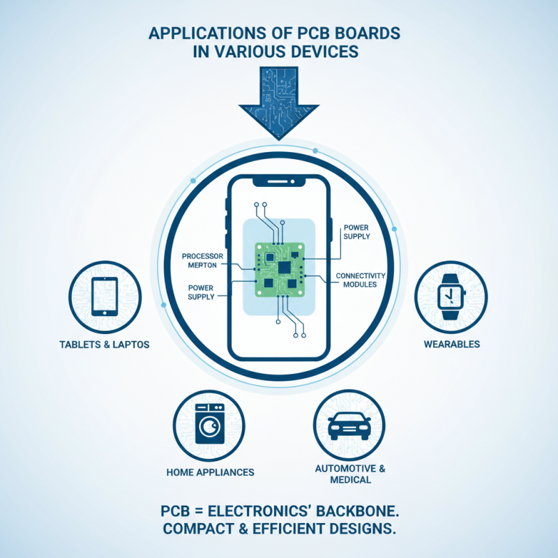
Applications of PCB Boards in Various Devices
PCB boards, or printed circuit boards, are crucial in modern electronics. They serve as the backbone for countless devices, from smartphones to home appliances. In a smartphone, a PCB connects the processor, memory, and power supply, ensuring smooth operation. These boards simplify complex circuits, allowing for compact and efficient designs.
In the realm of consumer electronics, PCB boards are invaluable. They are found in TVs, laptops, and gaming consoles, enabling connectivity and functionality. Each device typically contains multiple PCBs, each serving specific roles. In certain cases, a poorly designed PCB can lead to device failures, highlighting the importance of engineering expertise.
Industrial applications also rely on PCB technology. Machinery and control systems often utilize specialized PCBs for reliability. For example, in manufacturing equipment, PCBs ensure precision and consistency. However, despite advancements, challenges remain in PCB design, such as accommodating higher speeds and miniaturization. Engineers must continually innovate to meet these evolving demands.
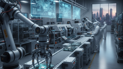
The Manufacturing Process of PCB Boards
The manufacturing process of PCB boards involves several key stages: design, material selection, fabrication, and assembly. Each step plays a crucial role in determining the board's functionality. For instance, a well-designed PCB can significantly enhance electrical performance. According to a market research report, the global PCB industry is projected to surpass $75 billion by 2025, highlighting its importance in electronics.
During fabrication, layers of copper and insulating material are meticulously arranged. High-pressure laminating machines apply heat to bond these layers. This process requires precision. Even minor errors can result in defective circuits. It's essential to maintain strict quality control measures at this stage.
*Tip: Always choose reliable suppliers for raw materials. Quality materials lead to better final products.*
Before assembly, meticulous testing is conducted. This helps identify any solder defects. In some cases, subpar designs can lead to failures in the final product. It's vital to review and refine designs continually.
*Tip: Regularly update your design practices. Technology evolves quickly in this industry.*
What is a PCB Board and How is it Used in Electronics? - The Manufacturing Process of PCB Boards
| Material |
Application |
Layer Count |
Manufacturing Process |
| FR-4 |
Consumer Electronics |
1-2 Layers |
Photoengraving, Etching |
| CEM-1 |
Home Appliances |
Single Layer |
Core Layer Lamination |
| Aluminum |
LED Lighting |
Double Layer |
Dielectric Layer Application |
| Flexible Materials |
Wearable Devices |
Multi-layers |
Printing, Lamination |