Our Commitment to a Greener Future


In the rapidly evolving landscape of electronics, mastering printed circuit board design is crucial for engineers and designers striving to enhance performance and reliability in their products. A printed circuit board (PCB) serves as the backbone of electronic devices, facilitating connections and ensuring seamless communication between components. As demands for miniaturization, efficiency, and function intensify, the intricacies of PCB design become increasingly significant. This article explores essential strategies and best practices that contribute to high-quality PCB design, focusing on ways to optimize layout, reduce interference, and improve manufacturability. By understanding the pivotal role of printed circuit board design in the development of innovative electronic solutions, professionals can elevate their projects to meet contemporary challenges and future trends in technology.
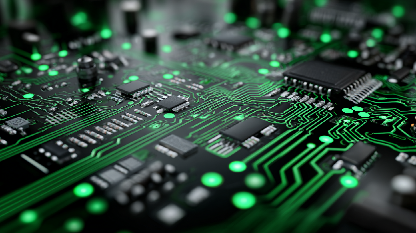
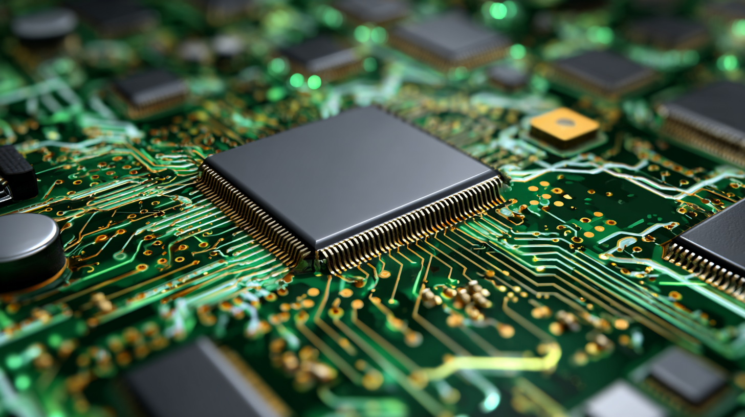
Printed Circuit Board (PCB) design is a critical skill for anyone looking to enhance electronics performance. At its core, understanding the design principles is essential for creating efficient and functional PCBs. A well-designed PCB not only supports the necessary electrical connections but also promotes efficient heat dissipation and minimizes electromagnetic interference. Designers should always place components strategically to optimize signal integrity and reduce noise.
Tips: When starting a PCB design, always keep component placement logical. Group related components together and ensure that power and ground traces are adequately sized to handle the required current. This minimizes voltage drops and ensures stable performance. Additionally, pay attention to the routing of traces; shorter and wider traces can significantly improve signal quality.
Another pivotal principle in PCB design is the importance of layers. Depending on the complexity of the circuit, using multiple layers can help manage signals better and reduce interference. Opt for a layered approach when you are handling high-speed signals or dense components.
Tips: Utilize vias judiciously to connect different layers, as excessive vias can cause signal degradation. Always follow standard design rules for layer stack-up, which aids in maintaining the electrical integrity of the circuit while ensuring manufacturability. Proper documentation and adherence to design guidelines will facilitate easier troubleshooting and modifications in the future.
Effective component placement and routing are crucial for optimizing printed circuit board (PCB) performance. According to a report by IPC, up to 30% of manufacturing costs can be attributed to inefficient PCB designs, underscoring the importance of maximizing routing efficiency. A well-structured layout not only enhances electrical performance but also reduces signal integrity issues, which are pivotal in high-frequency applications.
Tips: Ensure that components are placed logically; for instance, high-frequency signals should be routed first, with a focus on minimizing trace length. Additionally, grouping related components can facilitate better routing paths and simplify manufacturing processes. Aiming for a 50-60% routing efficiency can significantly decrease electromagnetic interference and improve overall circuit stability.
Moreover, utilizing advanced design software that includes simulation tools can enhance decision-making during the layout phase. A recent study indicated that designers using simulation tools experienced a 25% reduction in design errors, reinforcing the importance of integrating technology into the PCB design process. This integration not only streamlines the design workflow but also aids in achieving a higher first-pass yield in production, ultimately leading to enhanced electronics performance.
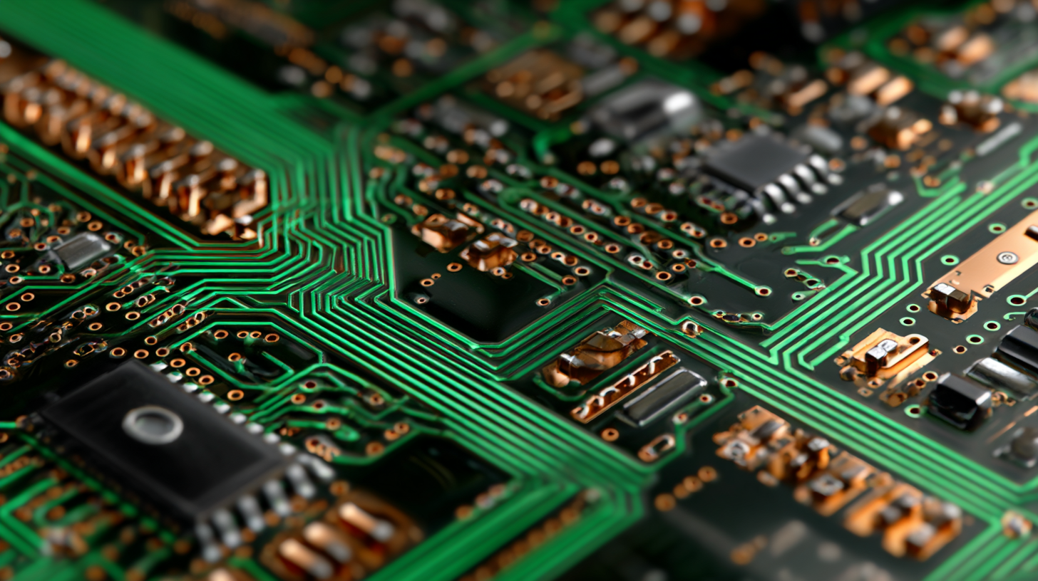
In modern electronics, maintaining signal integrity is paramount for enhancing the performance of printed circuit boards (PCBs). According to a report by the IPC (Institute of Printed Circuits), poor signal integrity can lead to increased electromagnetic interference (EMI) and crosstalk, which significantly degrade the functionality of electronic devices. Implementing best practices for layer stackup is essential to minimize these issues. For instance, a typical stackup might include alternating signal, ground, and power layers to create a controlled impedance environment, which helps in reducing noise and enhancing the overall performance of the PCB.
Another critical factor is the careful placement of components and traces. A study by the IEEE indicates that over 25% of PCB failures are attributed to improper signal routing. By optimizing trace lengths and maintaining consistent widths, designers can ensure minimal signal degradation. Additionally, using via stitching and ground planes can further improve signal integrity by providing low-impedance paths for return currents. These strategies, combined with advanced simulation tools, allow engineers to predict and mitigate potential issues before they occur, resulting in more reliable and high-performance electronic devices.
| Practice | Description | Impact on Signal Integrity | Recommended Layer Stackup |
|---|---|---|---|
| Controlled Impedance | Maintaining consistent impedance throughout the PCB. | Reduces signal reflections and increases performance. | 4-layer stack with differential pairs. |
| Proper Grounding | Using ground planes to minimize EMI. | Improves signal integrity by reducing noise. | 6-layer stack with internal ground layers. |
| Via Management | Optimizing via placement and type. | Minimizes signal loss and delay. | 4-layer stack using blind/buried vias. |
| Layer Segregation | Separating power and signal layers. | Enhances signal clarity and reduces noise coupling. | 8-layer stack with dedicated power and ground layers. |
| Decoupling Capacitors | Placing capacitors close to IC power pins. | Stabilizes power supply levels and reduces noise. | 4-layer stack with capacitors distributed across layers. |
Mastering printed circuit board (PCB) design is crucial for optimizing thermal management and power distribution in electronic devices. Effective thermal management can significantly enhance the reliability and performance of electronic systems. According to a report by IPC, nearly 40% of PCB failures are attributed to thermal issues, indicating the importance of adequate heat dissipation strategies in design. Techniques such as using thermal vias, dedicated ground planes, and optimizing component placement can help spread heat more evenly across the board, minimizing hotspots and prolonging device lifespan.
When it comes to power distribution, ensuring consistent voltage levels is critical for performance, particularly in high-demand applications. The IPC-2221 standard emphasizes the need for careful planning of power traces to reduce resistance and inductance, which can lead to power loss and signal integrity issues. Advanced techniques, such as implementing power islands and using wider traces for power distribution, can minimize voltage drops and improve overall efficiency. Data from a recent industry survey indicates that systems with optimized power distribution setups exhibit a 20% increase in operational efficiency, underscoring the benefits of strategic PCB design for enhanced electronic performance.
In the modern landscape of electronics, the design of printed circuit boards (PCBs) is critical for achieving optimal performance. Utilizing advanced software tools is essential for streamlining the PCB design workflow, as they help engineers efficiently manage complex layouts and intricate circuitry. Programs like Altium Designer and KiCAD offer features such as schematic capture, electronic component libraries, and design rule checks, ensuring that designers can focus on innovation while minimizing errors.
Moreover, these software tools enable collaboration among team members, facilitating real-time feedback and modifications. With capabilities for 3D visualization, engineers can better assess spatial constraints and component placements before production, reducing the likelihood of costly revisions. The implementation of automated routing and signal integrity analysis further enhances efficiency, allowing designers to optimize their designs for factors like electromagnetic interference and thermal performance. By leveraging these software solutions, engineers can not only streamline their workflow but also elevate the overall quality and reliability of their PCB designs.
