Top Tips for Effective Printed Circuit Board Design
Effective printed circuit board design is a crucial aspect of electronics. It directly influences the performance and reliability of devices. A well-designed PCB ensures efficient signal transmission and energy use.
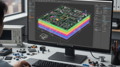
Many factors contribute to successful PCB design. Layout choices, material selection, and component placement all require careful consideration. Designers often face challenges. Overcrowded layouts can cause signal interference. Improper grounding can lead to performance issues.
Learning and improving in printed circuit board design is an ongoing process. Each project presents unique challenges and opportunities. Reflecting on past designs helps in identifying areas for improvement. The goal is to enhance performance while keeping costs reasonable.
Key Principles of PCB Layout to Minimize Signal Interference
Effective PCB layout is crucial for minimizing signal interference. As electronic devices become more complex, the risk of noise and crosstalk increases. A report by IPC states that poor layout can lead to signal integrity issues in over 45% of designs. Designers must prioritize component placement and routing techniques.
Proper grounding techniques are essential. A ground plane reduces electromagnetic interference, yet many designers overlook it. Studies show that grounding errors contribute to nearly 35% of performance issues. Ensuring a solid connection between the ground and components makes a significant difference.
In addition, using shorter traces can minimize inductance and capacitance. This evidently improves signal quality. The ideal trace length should be reviewed regularly. Some designs show traces that could be much shorter. Regular evaluations of layout choices can help prevent future signal integrity problems. A well-thought-out approach leads to better overall performance in circuit boards.
Understanding the Role of Ground Planes in PCB Design
Ground planes play a critical role in PCB design, influencing both functionality and performance. They act as a reference point for signals and help mitigate noise. According to a report by IPC, effective ground planes can reduce electromagnetic interference (EMI) by up to 30%. This reduction is vital for maintaining signal integrity in high-speed circuits.
When designing a PCB, engineers often overlook the significance of the ground plane layout. A poorly placed ground plane can lead to performance issues. For instance, if the ground plane is split or disconnected, it may create ground loops. These loops can introduce noise and compromise the system's reliability. A study published in the IEEE Transactions on Components, Packaging, and Manufacturing Technology highlighted how 15% of PCB design errors stem from ground-related issues.
Choosing the right materials for ground planes is also crucial. While copper is common, using different thicknesses can impact performance. Thin ground planes may lead to higher resistance, which results in voltage drops. Conversely, thicker planes are more robust but add weight. It's essential to strike a balance. Mistakes in this area can lead to suboptimal performance and increased costs during production.
Optimizing Trace Width and Spacing for Current Carrying Capacity
In printed circuit board (PCB) design, trace width and spacing are critical factors for ensuring optimal current carrying capacity. According to IPC-2221 standards, the trace width must be calculated based on the expected current and acceptable temperature rise. A common rule of thumb is that a 1 oz/ft² copper layer can safely carry approximately 1 amp per 10 mil (0.01 inch) of trace width. This guideline can help prevent overheating and potential circuit failure.
Actual design scenarios often reveal challenges. Designers sometimes underestimate the effects of ambient temperature and insulation types. For instance, a PCB operating in a high-temperature environment may require wider traces than those calculated under standard conditions. A 2008 IPC report indicated that improper trace sizing led to a 30% increase in failures for industrial PCBs. These insights highlight the need for designers to thoroughly analyze their specific application and environment.
Spacing is equally important. Insufficient spacing can lead to short circuits or signal integrity issues. A common misconception is that wider traces can compensate for tighter spacing. However, this approach can create additional problems, such as increased electromagnetic interference. Designers should refer to resources like IPC-2152 for guidance on operational limits in complex layouts. Reflection on past mistakes can greatly enhance future designs.
Optimizing Trace Width and Spacing for Current Carrying Capacity
Incorporating Design for Manufacturability (DFM) in PCB Projects
Design for Manufacturability (DFM) is essential in PCB design. It ensures that your printed circuit boards are not only functional but also easy to produce. One key aspect of DFM is minimizing complexity.
Complex designs are harder to manufacture. Simple, elegant designs can lead to fewer errors during production.
Incorporating proper spacing is another vital consideration. Ensure components have enough room for soldering.
Overcrowded layouts can lead to manufacturing delays. Small mistakes in tight spaces often result in significant costs. Another area to focus on is the choice of materials. Not all components are created equal. Some are more difficult to work with. This might lead to production hiccups later.
It's also crucial to collaborate with your manufacturing partner early. Their insights can guide your design choices. They may identify potential production issues before they escalate. However, rushing this stage can result in overlooking vital factors.
Review design files rigorously and invite feedback. These steps are necessary for a seamless manufacturing process. DFM has a clear impact on overall project success.