2026 Best PCB Fabrication and Assembly Processes for Your Projects?
In the fast-evolving world of electronics, choosing the right methods for PCB fabrication and assembly has never been more crucial. The year 2026 promises significant advancements in these processes. Businesses must stay updated to meet growing demands. As projects increase in complexity, the choice of materials and techniques becomes vital. Every decision impacts the final product's performance and reliability.
Conducting comprehensive research on PCB fabrication and assembly is essential. Innovations emerge frequently, and what worked a year ago may no longer be optimal. Companies may find themselves in a challenging position if they do not adapt. Relying on outdated methodologies can lead to costly mistakes. Understanding current trends can drive success and help avoid pitfalls.
However, not every technique fits every project perfectly. Some processes may yield great results but can be expensive or time-consuming. It's necessary to balance efficiency and cost. Skilled professionals must evaluate the unique needs of each project. Striking the right balance may take time and detailed consideration. This ongoing reflection on methods will define the future of PCB fabrication and assembly.

Overview of PCB Fabrication and Assembly Processes in 2026
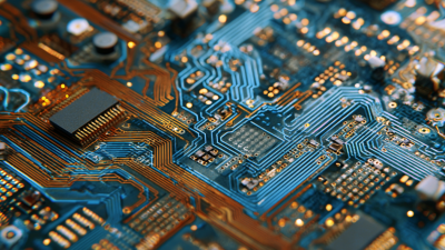
The year 2026 brings advancements in PCB fabrication and assembly processes, shaping the landscape of electronics manufacturing. A report by Smith & Associates highlights that the global PCB market is projected to reach $100 billion, driven by innovations in technology and increasing device complexity. This growth demands more efficient and precise fabrication techniques.
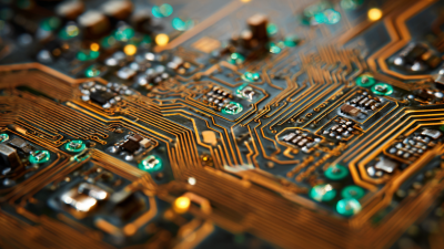
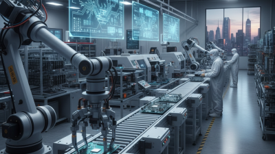
Current trends showcase the rise of additive manufacturing in PCB production. This approach allows for intricate designs and reduced waste. However, it also promotes challenges in standardization and scalability. As fabricators embrace machine automation, some struggle with integration. Effective collaboration between design and engineering teams is necessary to overcome these issues.
Assembly processes are evolving, too. With the rise of smaller components, traditional methods face limitations. A study by PCB Magazine points out that 35% of companies report difficulties with microchip handling. This underscores a need for improved training and equipment. As manufacturers strive for higher yields, they must remain vigilant about quality control. Mistakes can lead to significant financial losses and impact product reliability. The focus on innovation must not overshadow the importance of process refinement and workforce development.
2026 Best PCB Fabrication and Assembly Processes Overview
This chart illustrates the production efficiency percentages of different PCB fabrication and assembly processes in 2026. The data indicates that Process C has the highest efficiency, while Process D has the lowest efficiency among the evaluated options.
Key Technologies Influencing PCB Fabrication and Assembly
The landscape of PCB fabrication and assembly is rapidly evolving.
Key technologies are significantly influencing processes in this sector.
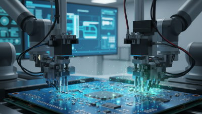
For instance, advancements in automation have proven effective in improving production efficiency.
Reports indicate that automated systems can reduce labor costs by up to 30%.
However, over-reliance on automation may lead to quality control issues.
The implementation of AI in PCB design is also noteworthy.
AI algorithms can optimize layouts and predict potential failures.
Research shows that AI-enhanced processes can increase yields by as much as 20%.
Yet, there remains a risk of losing the human element in critical design decisions.
Balancing technology and expert insight is essential but often challenging.
Moreover, the trend towards smaller, more complex PCBs introduces challenges in assembly processes.
With components shrinking, precision becomes paramount.
Recent studies suggest that improper alignment can lead to a
15% increase in defects.
Companies must invest in high-quality inspection technologies to mitigate these risks. Failing to address these aspects could undermine technological advancements in PCB fabrication.
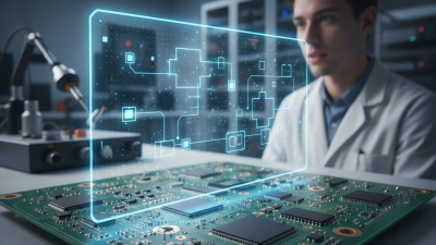
Step-by-Step Guide to PCB Design for Optimal Manufacturing
Creating a PCB design involves several crucial steps. Begin by defining your project requirements. Determine the size, shape, and layer count of your PCB.
Sketch your circuit diagram to visualize connections and components. This stage may feel overwhelming. Don’t rush through it. Mistakes at this phase can lead to costly changes later.
Next, it’s time to choose a design software. Many options are available, each with unique strengths and weaknesses. Some software may seem user-friendly but lack advanced features.
Take your time to explore possibilities. You might discover a tool that fits perfectly. Remember to create a draft layout after placing components. Consider trace width and spacing carefully. These details significantly affect performance.
Finally, prepare your design for manufacturing. Double-check all connections and component placements. Use the design rule check feature to catch errors. It's easy to overlook small mistakes. Even experienced designers make them.
Share your design with colleagues for feedback. Their insights could be invaluable. This collaborative approach often reveals overlooked issues. Embracing this process means learning continuously, making your future designs even better.
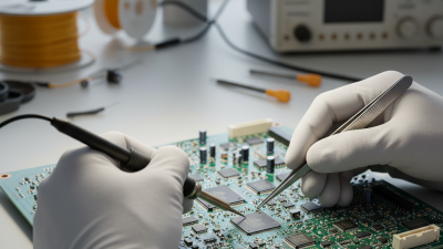
Quality Assurance Practices in PCB Production and Assembly
Quality assurance in PCB production is crucial for maintaining high standards. This phase involves rigorous testing and inspection. Engineers often use automated and manual methods to ensure each board meets specifications. Common methods include visual inspections, electrical testing, and thermal cycling.
Regular audits of manufacturing processes can help identify potential flaws. Workers should be trained to recognize defects and anomalies. Implementing a feedback loop with suppliers can enhance quality. Adjustments made based on feedback can reduce error rates in future batches.
Tips for improving quality include conducting thorough pre-production reviews. Use statistical process control to monitor production metrics. Consistent communication among team members can prevent misunderstandings. Always document changes in the fabrication process, even minor ones, as they might impact quality. Each mistake offers a chance for growth and improvement, creating a culture focused on excellence.