In 2026, global buyers will face a wider range of PCB fab options than ever before. Standard multilayer boards remain practical for industrial controls, networking equipment, and consumer devices. HDI fabrication supports compact products with fine traces and microvias. Rigid-flex boards can reduce connectors, wiring space, and assembly steps. High-frequency materials serve radar, telecommunications, and other signal-sensitive applications. Each type solves a different engineering problem. None is universally superior.
Choosing a supplier requires more than comparing a quoted price. Buyers should examine layer capability, minimum trace width, via technology, material control, impedance testing, and production capacity. A reliable pcb fab should provide clear stack-up data, inspection records, sample evidence, and realistic delivery commitments. Ask about solder-mask registration. Review cross-section reports. Request references for similar projects. These details often reveal more than a polished website.
Experience also shows that the cheapest offer may become expensive after redesigns, yield losses, or delayed approvals. However, premium pricing does not automatically prove better quality. That assumption deserves review. Regional sourcing, certification needs, shipping routes, and technical communication can change the final decision. Buyers should compare total ownership cost, not only the factory quotation. They should also confirm whether prototypes and mass production use consistent materials and processes. A careful evaluation can reduce surprises, although no supplier comparison is completely risk-free. This guide examines leading PCB fabrication types and explains where each option may fit global purchasing plans in 2026.

PCB fabrication types differ in materials, layer construction, routing density, and assembly behavior. For global buyers, comparison starts inside the pressing, drilling, plating, and inspection stages.
Rigid PCBs Rigid PCBs use glass-reinforced epoxy laminates and remain stable during automated assembly. Multilayer versions add sequential lamination, inner-layer alignment, and plated-through holes. This improves routing capacity but increases registration risk. Rigid boards stay flat.
Flexible PCBs Flexible PCBs use polyimide films, copper foil, and protective coverlay. The circuit bends, but repeated movement requires controlled bend radius and accurate copper treatment.
Rigid-Flex Boards Rigid-flex boards combine both structures through bonded transitions. These designs reduce connectors, yet demand careful stack-up control and stricter testing.
HDI Boards HDI boards use fine traces, microvias, and sequential build-up layers. Microvias save space. They also raise drilling and reliability requirements.
Metal-Core PCBs Metal-core PCBs move heat toward an aluminum or copper base, making them useful for high-power lighting and thermal applications.
High-Frequency Boards High-frequency boards require controlled dielectric properties, smoother copper, and precise impedance management.
During supplier evaluation, request cross-section reports, material certificates, capability data, and sample testing. A low layer count does not always mean lower manufacturing risk.
I have seen simple-looking boards fail because plating thickness was treated as an afterthought. That lesson still deserves attention.
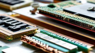
Rigid PCB Fabs for Standard, High-Volume Electronic Products
Rigid PCB fabrication remains the practical choice for appliances, industrial controls, automotive modules, and everyday consumer electronics. Prismark’s 2024 industry forecast estimated global PCB sales could approach 100 billion US dollars by 2028, supported by steady demand for conventional multilayer boards. These products usually need predictable dimensions, stable dielectric performance, and repeatable drilling. Not exotic materials.
A qualified rigid PCB fab should control copper thickness, layer registration, solder-mask coverage, and final electrical testing across long production runs. IPC’s 2024 PCB industry data also indicated continuing pressure on order volumes and pricing, making process stability more valuable than impressive prototypes. In factory audits, small details matter: clean drill walls, readable lot codes, and flat panels reduce avoidable assembly delays. However, high volume can hide weaknesses. A supplier may pass early samples but struggle after thousands of panels. That risk deserves attention. Buyers should review capability reports, first-article records, defect trends, and corrective-action history before approving production. The cheapest quotation can become expensive when yield falls. Some specifications also need reconsideration; unnecessary tight tolerances may increase cost without improving the finished product. A clear stack-up, realistic tolerance window, and documented inspection plan usually create a stronger purchasing decision.
Typical finished layer-count ranges used in high-volume rigid PCB programs. Lower-layer boards are common for cost-sensitive products, while higher-layer boards support greater routing density and electrical functionality.
Standard rigid PCB fabrication is widely used for consumer appliances, computing peripherals, industrial controls, automotive electronics, and telecom equipment. The ranges shown are common industry design windows rather than company-specific production data.
2026 Top PCB Fab Types for Global Buyers?
Flexible and rigid-flex PCB fabrication is becoming central to compact electronics. Flexible circuits fold around batteries, cameras, and hinged assemblies. Rigid-flex designs combine stable component zones with dynamic bending areas. This can reduce connectors, wiring, and assembly space. Space is expensive.
Fortune Business Insights valued the global flexible printed circuit board market at approximately USD 27.27 billion in 2023. Its 2024–2032 report projects growth toward USD 57.22 billion by 2032. These figures show strong demand, but forecasts are not purchase orders.
Buyers still need evidence from the actual factory. Ask for bend-cycle results, dimensional capability, impedance data, and material traceability. Small errors matter.
A capable flex or rigid-flex fab should control copper thickness, coverlay registration, adhesive flow, and minimum bend radius. IPC’s 2024 PCB industry reporting also indicates continuing pressure on production quality and supply-chain responsiveness. Therefore, global buyers should review first-article inspection records and process capability studies before scaling production.
A rigid-flex stackup may look correct in CAD yet fail after repeated bending. That uncomfortable gap deserves attention.
Request sample panels, cross-sections, thermal testing, and documented design-for-manufacturing feedback. The best supplier is not always the one offering the lowest quotation. Reliable communication and repeatable process control often protect compact designs better.
Advanced PCB fabs are shifting from basic multilayer production toward high-speed and high-density structures. Prismark’s 2024 market review estimates global PCB revenue at about $74 billion for 2024, with computing and communication hardware driving demand. Those applications require tighter impedance control, finer lines, and stronger thermal management.
High-speed fabs commonly use low-loss laminates, sequential buildup, laser microvias, and advanced back drilling. High-density interconnect boards can place microvias beneath components, saving routing space on compact modules. IPC’s 2024 PCB Technology Roadmap emphasizes signal integrity, power delivery, and reliability as major design challenges. A practical fab should therefore control dielectric thickness within narrow tolerances and verify impedance through test coupons.
The details matter.
For global buyers, fabrication evidence is more useful than polished claims. Ask for cross-section data, copper roughness measurements, solderability results, and thermal cycling records. IPC-6012 qualification requirements can help compare rigid-board capabilities across regions. SEMI’s 2024 semiconductor equipment report also points to continued investment in advanced computing infrastructure, increasing pressure on PCB density and power handling.
Yet, higher density is not automatically better. Tiny vias can reduce flexibility during repair, and advanced laminates may increase scrap rates. Some supplier roadmaps look impressive but lack long-term field data. I would request sample builds before approving volume production. That step costs time, but skipping it can expose hidden process weaknesses.
Global buyers compare PCB fabs by more than board type. Rigid, flex, rigid-flex, and HDI factories serve different design risks. A four-layer rigid board may need stable impedance and clean solder mask registration. A flex circuit demands controlled bending tests, copper adhesion data, and careful coverlay placement. For HDI, buyers should examine laser-via capability, stacked-via reliability, and microsection reports. Ask for recent first-article records, not polished presentation slides. Quality evidence should include AOI results, electrical testing, capability studies, and lot traceability. Small details matter. A missing test record can signal weak process control.
Cost comparisons require the same drawing, material stack-up, quantity, and delivery target. Otherwise, a cheaper quote may simply exclude testing, tooling, or packaging. Request separate pricing for prototypes, volume production, engineering changes, and expedited orders. Then compare yield assumptions, not only the unit price. Compliance deserves equal attention. Reliable fabs should provide current declarations for RoHS, REACH, conflict-minerals reporting, and applicable safety requirements. They should also explain how restricted substances are controlled during incoming inspection. Site audits can verify calibration labels, humidity controls, chemical storage, and worker training. Yet audits are snapshots. A supplier may pass one visit and disappoint six months later. That uncomfortable gap deserves a corrective-action plan, regular sampling, and clear escalation rules. Buyers should document every assumption before awarding production.
| PCB Fab Type | Typical Applications | Representative Technical Range | Relative Cost Index | Typical Production Lead Time | Main Quality Evaluation Points | Compliance and Buyer Verification Focus |
|---|---|---|---|---|---|---|
| Standard 2-Layer Rigid PCB | Consumer electronics, simple control boards, power adapters, lighting, and low-density industrial products. |
1.0–1.6 mm finished thickness; approximately 0.15–0.25 mm trace and space; standard FR-4 construction. |
1.0–1.3 Baseline reference |
5–10 working days for standard production; expedited service may be shorter. | Dimensional accuracy, solderability, hole quality, copper thickness, dielectric integrity, and electrical test coverage. | Confirm IPC-6012 or equivalent requirements, material traceability, electrical testing, restricted-substance controls, and applicable product-safety requirements. |
| 4–6 Layer Multilayer Rigid PCB | Industrial controls, embedded computing, automotive modules, networking equipment, and medium-density electronics. |
Approximately 0.10–0.20 mm trace and space; controlled impedance available; sequential lamination may be used for advanced designs. |
1.4–2.2 | 10–18 working days, depending on material, layer count, and testing requirements. | Layer registration, lamination quality, copper distribution, impedance control, via reliability, CAF risk, and thermal-stress performance. | Verify IPC-6012 class, impedance test reports, microsection records, material certificates, process-change control, and ISO 9001-based quality management. |
| High-Layer-Count Rigid PCB | Servers, telecommunications equipment, medical systems, aerospace electronics, and complex industrial platforms. |
Commonly 8–20+ layers; fine-pitch routing and controlled impedance; high-density power and signal distribution. |
2.0–4.5 | 15–30 working days for production, with engineering review often required before release. | Registration across all layers, low-loss material behavior, via fatigue life, resin fill, warpage, impedance uniformity, and defect escape rate. | Request process qualification, cross-section data, reliability testing, supplier-change notification, traceability, and documentation for sector-specific quality systems. |
| HDI Microvia PCB | Smart devices, compact computing products, wearable electronics, cameras, and miniaturized medical equipment. |
Laser microvias, blind and buried vias; approximately 0.075–0.15 mm line and space in advanced builds; sequential build-up structures. |
2.5–5.0 | 15–28 working days, depending on build-up cycles and microvia testing. | Microvia integrity, via stacking reliability, pad cratering, fine-line yield, resin recession, solder-mask registration, and warpage. | Verify IPC-6012 HDI provisions or equivalent specifications, microsection sampling, thermal-cycle results, laser-drill control, and process capability data. |
| Flexible PCB | Displays, cameras, sensors, battery interconnects, medical wearables, automotive harness replacement, and compact moving assemblies. |
Polyimide-based constructions are common; one to several conductive layers; dynamic or static-bend designs require different qualification criteria. |
2.0–5.0 | 15–30 working days; stiffeners, coverlay, and forming operations can extend the schedule. | Bend-cycle life, conductor-to-substrate adhesion, coverlay registration, flex-zone cleanliness, dimensional stability, and connector durability. | Confirm IPC-6013 or equivalent requirements, bend-cycle validation, material flammability evidence, chemical restrictions, and full lot traceability. |
| Rigid-Flex PCB | Aerospace systems, medical instruments, industrial robotics, high-reliability controls, and assemblies requiring reduced connectors. |
Combined rigid and flexible zones; multilayer structures with controlled bend areas; customized bend radius and stiffener design. |
3.5–8.0 | 20–40 working days because of complex lamination, forming, and inspection requirements. | Rigid-to-flex transition reliability, bend-radius compliance, layer registration, delamination resistance, conductor fatigue, and dimensional repeatability. | Verify IPC-6013-based qualification, thermal and mechanical cycling, first-article inspection, configuration control, material traceability, and sector-specific certification needs. |
| Metal-Core PCB | LED lighting, automotive power electronics, motor controls, power supplies, and applications requiring heat dissipation. |
Aluminum or copper base plate; thermally conductive dielectric layer; typically one to several copper circuit layers. |
1.5–3.5 | 8–18 working days for standard constructions; custom thermal stacks may require longer engineering time. | Thermal resistance, dielectric breakdown strength, base-plate flatness, copper adhesion, thermal cycling, and solder-joint fatigue. | Request thermal-conductivity data, dielectric withstand results, flammability information, material declarations, and confirmation of the required IPC performance class. |
| High-Frequency or High-Speed PCB | Wireless communications, radar, automotive sensing, high-speed computing, test equipment, and RF modules. |
Low-loss or very-low-loss laminates; controlled impedance and tight dielectric tolerances; specialized surface finish and stack-up control. |
2.5–6.0 | 15–30 working days, subject to material availability and impedance-control requirements. | Dielectric consistency, insertion loss, impedance accuracy, surface roughness, glass-weave effects, drill quality, and signal-integrity performance. | Verify laminate data sheets, lot-based dielectric values, impedance coupons, test frequency, material traceability, and controlled storage and handling procedures. |
| Heavy-Copper PCB | Battery systems, power converters, industrial drives, renewable-energy equipment, and high-current distribution. |
Commonly 2–6 oz copper, with heavier copper available; enlarged vias and wider conductors; increased thermal and current-carrying capacity. |
2.0–5.0 | 12–25 working days because of etching, plating, lamination, and thermal-management complexity. | Copper thickness uniformity, conductor edge quality, plated-hole reliability, thermal rise, dielectric clearance, and solderability. | Confirm copper-thickness measurements, thermal testing, electrical safety spacing, material flammability data, and inspection criteria for high-current applications. |
| RF and Microwave Hybrid PCB | Antennas, satellite communications, radar, navigation, specialized wireless equipment, and precision instrumentation. |
Hybrid dielectric stack-ups may combine different material families; controlled impedance and low-loss routing; tight mechanical and electrical tolerances. |
4.0–9.0 | 20–45 working days, including material review, stack-up approval, and specialized testing. | Material compatibility, dielectric stability, conductor roughness, registration between material systems, RF loss, and environmental performance. | Require material certificates, RF test methodology, controlled stack-up documentation, thermal-cycle data, process-change notification, and end-use regulatory review. |
Buyer note: Cost indices and lead times are indicative industry benchmarks rather than fixed quotations. Actual results vary with order volume, panel utilization, materials, surface finish, testing, tolerances, geographic logistics, and qualification requirements. Compliance should be verified from current certificates, test reports, and production-lot records rather than inferred from PCB type alone.